Why LDS Antennas Became the Mainstream in Compact Consumer Electronics
This article explores why LDS antennas consumer electronics designs have become the mainstream choice in modern compact devices.
It analyzes antenna form factor evolution, structural constraints, and manufacturing realities that drive LDS adoption in space-constrained, multi-band products.
The discussion focuses on practical engineering trade-offs rather than theoretical antenna models.
Table of Contents
- Foreword
- What is RF? Why is an Antenna Essential?
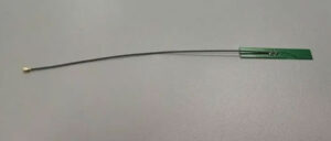
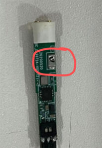
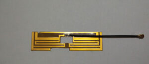
- The Four Most Common Antennas in Consumer Electronics
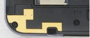
- Why Have LDS Antennas Become the Mainstream Solution?
- Structural Forms and Design Considerations of LDS Antennas
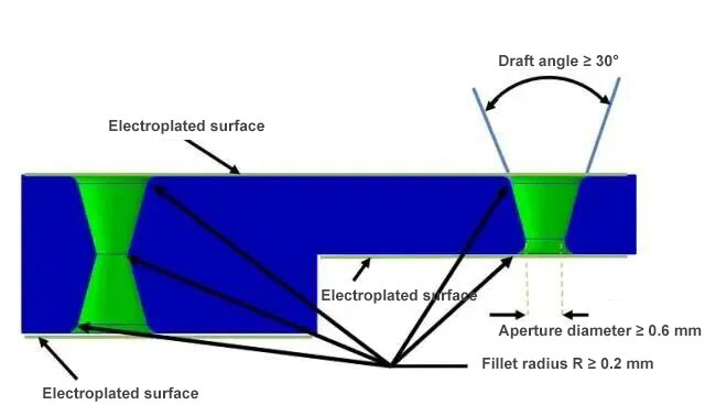
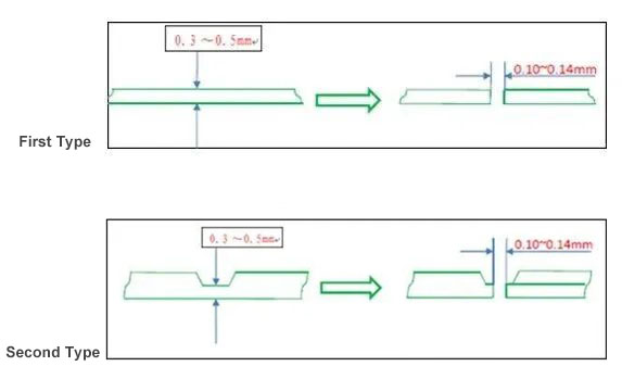
- Key Considerations for LDS Process
- LDS Material System and Selection Logic
- Conclusion